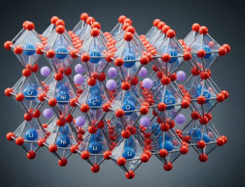
chromium oxide green in Advanced semiconductor polishing: Precision Beyond Nanometers
Introduction
The semiconductor industry stands at the precipice of a technological revolution. As we transition from 3nm to 2nm and beyond, the demand for ultra-precision polishing materials has never been more critical. chromium oxide green (Cr₂O₃), a material that has served the abrasive industry for decades, is now experiencing a renaissance in advanced semiconductor manufacturing. This article explores the sophisticated applications of chromium oxide green in semiconductor polishing, examining how this material enables the production of next-generation chips with atomic-level precision.
The Challenge of Modern semiconductor Manufacturing
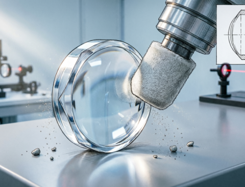
Modern semiconductor fabrication requires polishing processes that can achieve surface roughness below 0.5 nanometers (Ra < 0.5 nm). This is not merely a matter of making surfaces smoother—it is about creating atomically flat surfaces that determine the performance, reliability, and yield of semiconductor devices.
Traditional polishing materials, including silicon carbide and aluminum oxide, have reached their practical limits. They tend to create subsurface damage, generate excessive heat, and produce inconsistent results across large wafer surfaces. The semiconductor industry needed a material that could:
1. Achieve ultra-low surface roughness without subsurface damage
2. Maintain consistent polishing rates across 300mm wafers
3. Provide selective polishing between different materials (copper, tungsten, dielectric layers)
4. Generate minimal heat during the polishing process
5. Produce predictable, repeatable results for high-volume manufacturing
chromium oxide green emerged as the solution to these challenges, but not through simple application of existing technology. Instead, semiconductor manufacturers have developed sophisticated polishing slurries and processes specifically engineered around chromium oxide green‘s unique properties.
The Science Behind chromium oxide green polishing
chromium oxide green possesses several characteristics that make it ideal for semiconductor applications:
Hardness and Particle Size Distribution: chromium oxide green has a Mohs hardness of 8.5-9, making it harder than most materials it polishes. However, the key innovation lies in particle size control. Modern semiconductor polishing uses chromium oxide green particles in the 50-200 nanometer range, far smaller than traditional abrasives. This nano-scale particle size enables:
- Removal of material at the atomic level
- Minimal subsurface damage (typically < 5 nanometers)
- Smooth, predictable polishing rates
- Reduced defect density in polished surfaces
Chemical Inertness: Unlike some abrasives that react with polishing slurry components or the materials being polished, chromium oxide green remains chemically stable across a wide pH range (pH 2-12). This stability is crucial because semiconductor polishing slurries contain complex chemical additives designed to:
- Enhance selectivity between different materials
- Prevent corrosion of copper interconnects
- Control dishing and erosion
- Maintain consistent polishing rates
Thermal Properties: chromium oxide green has excellent thermal conductivity compared to other abrasives. During the high-speed polishing process (typically 100-300 rpm for wafer rotation), friction generates significant heat. chromium oxide green‘s thermal properties help dissipate this heat, preventing:
- Thermal damage to the wafer surface
- Degradation of photoresist patterns
- Uneven polishing rates due to thermal gradients
- Potential wafer warping
Real-World Application: CMP in 3nm Node Manufacturing
Consider the specific challenge of polishing copper interconnects in a 3nm node semiconductor process. The wafer contains:
- Copper interconnects with feature sizes as small as 20 nanometers
- Dielectric layers (typically low-k materials) that are softer than copper
- Tungsten vias connecting different metal layers
- Tantalum barrier layers
Traditional polishing would create significant dishing (over-polishing of copper) and erosion (under-polishing of dielectric areas). The solution involves a multi-step CMP process using chromium oxide green-based slurries:
Step 1: Bulk Copper Removal
A coarser chromium oxide green slurry (150-200 nm particles) removes excess copper quickly while maintaining selectivity over the dielectric. The polishing rate is approximately 300-400 nm/min for copper, compared to 50-80 nm/min for the dielectric.
Step 2: Copper Planarization
A medium-grade slurry (100-150 nm particles) refines the surface, achieving better uniformity across the wafer. polishing rates drop to 150-200 nm/min for copper, allowing better control.
Step 3: Final Polish
A fine chromium oxide green slurry (50-100 nm particles) achieves the final surface finish. At this stage, polishing rates are only 20-50 nm/min, but the surface roughness drops below 0.3 nm Ra, and subsurface damage is minimized.
The entire process, from bulk copper removal to final polish, takes approximately 45-60 seconds per wafer. For a 300mm wafer, this represents polishing an area of approximately 70,000 mm² to atomic-level precision.
Advanced Selectivity and Material-Specific polishing
One of the most sophisticated applications of chromium oxide green involves achieving selectivity between different materials on the same wafer. This is accomplished through careful formulation of the polishing slurry:
Copper-to-Dielectric Selectivity: By adjusting the pH, oxidizer concentration, and corrosion inhibitor levels, manufacturers can achieve selectivity ratios of 3:1 or higher. This means copper polishes three times faster than the dielectric, allowing precise control of the endpoint.
Tungsten polishing: Tungsten vias require different chemistry than copper. chromium oxide green slurries for tungsten polishing use different oxidizers and chelating agents, achieving polishing rates of 100-150 nm/min while maintaining selectivity over surrounding materials.
Barrier Layer Protection: Tantalum and tantalum nitride barrier layers must be protected during polishing. chromium oxide green slurries can be formulated to achieve selectivity ratios of 10:1 or higher between copper and barrier layers, ensuring barrier integrity.
Challenges and Solutions in semiconductor-Grade chromium oxide green
The transition from traditional abrasive applications to semiconductor polishing has revealed new challenges:
Particle Size Distribution Control: semiconductor-grade chromium oxide green requires extremely tight particle size distribution. While traditional abrasives might accept a range of 50-500 nm, semiconductor applications require 90% of particles within a 50-150 nm window. This necessitates advanced classification techniques and quality control.
Contamination Management: Even trace amounts of iron, silica, or other contaminants can cause defects in semiconductor devices. semiconductor-grade chromium oxide green must meet purity standards of 99.95% or higher, with specific limits on individual contaminants.
Consistency Across Batches: semiconductor manufacturers require batch-to-batch consistency within ±5% for polishing rates. This demands sophisticated manufacturing processes and real-time quality monitoring.
Environmental and Safety Considerations
chromium oxide green is chemically stable and non-toxic in its oxidized form (Cr³⁺). However, semiconductor manufacturing facilities must implement proper handling procedures:
- Dust control during slurry preparation
- Proper disposal of spent polishing slurries
- Worker safety protocols for handling fine particles
- Environmental compliance with local regulations
The Future of chromium oxide green in semiconductor Manufacturing
As the semiconductor industry moves toward 2nm and sub-2nm nodes, the role of chromium oxide green will likely expand:
1. Extreme Ultraviolet (EUV) Lithography: EUV processes create even more demanding surface requirements. chromium oxide green-based slurries are being developed specifically for EUV-patterned wafers.
2. 3D NAND Flash: As 3D NAND stacks reach 200+ layers, polishing becomes increasingly complex. chromium oxide green enables the precise control needed for these multi-layer structures.
3. Advanced Packaging: Chiplet-based designs require ultra-precise polishing of bonding surfaces. chromium oxide green is becoming essential for these applications.
4. Quantum Computing: Quantum devices require atomically smooth surfaces. Research is underway to develop chromium oxide green slurries specifically for quantum device fabrication.
Conclusion
chromium oxide green represents far more than a traditional abrasive material in semiconductor manufacturing. It is a precision tool that enables the creation of next-generation semiconductor devices. Through careful formulation, process control, and quality management, chromium oxide green-based polishing slurries achieve atomic-level precision while maintaining the consistency and reliability required for high-volume manufacturing.
As semiconductor technology continues to advance, chromium oxide green will remain at the forefront of polishing innovation, enabling the creation of faster, more powerful, and more efficient semiconductor devices. The material’s unique combination of hardness, chemical stability, and thermal properties makes it indispensable for the semiconductor industry’s continued progress toward ever-smaller, more capable chips.
For semiconductor manufacturers, material suppliers, and equipment makers, understanding the sophisticated applications of chromium oxide green is essential for maintaining competitive advantage in the rapidly evolving semiconductor landscape.